
Most ebook files are in PDF format, so you can easily read them using various software such as Foxit Reader or directly on the Google Chrome browser.
Some ebook files are released by publishers in other formats such as .awz, .mobi, .epub, .fb2, etc. You may need to install specific software to read these formats on mobile/PC, such as Calibre.
Please read the tutorial at this link. https://ebooknice.com/page/post?id=faq
We offer FREE conversion to the popular formats you request; however, this may take some time. Therefore, right after payment, please email us, and we will try to provide the service as quickly as possible.
For some exceptional file formats or broken links (if any), please refrain from opening any disputes. Instead, email us first, and we will try to assist within a maximum of 6 hours.
EbookNice Team

Status:
Available0.0
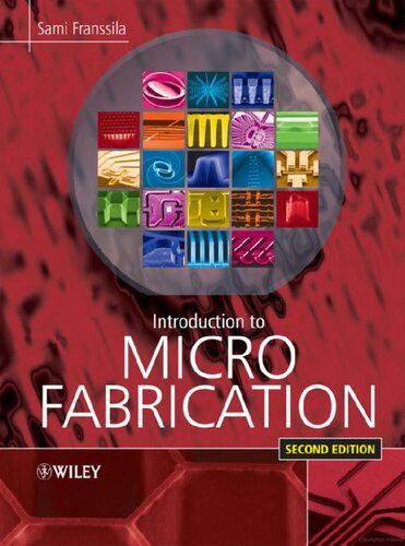
0 reviews(Ebook) Introduction to Microfabrication 2nd Edition by Sami Franssila - Ebook PDF Instant Download/Delivery: 9780470749838 ,0470749830
Full download (Ebook) Introduction to Microfabrication 2nd Edition after payment

Product details:
ISBN 10: 0470749830
ISBN 13: 9780470749838
Author: Sami Franssila
This accessible text is now fully revised and updated, providing an overview of fabrication technologies and materials needed to realize modern microdevices. It demonstrates how common microfabrication principles can be applied in different applications, to create devices ranging from nanometer probe tips to meter scale solar cells, and a host of microelectronic, mechanical, optical and fluidic devices in between. Latest developments in wafer engineering, patterning, thin films, surface preparation and bonding are covered.
This second edition includes:
With clear sections separating basic principles from more advanced material, this is a valuable textbook for senior undergraduate and beginning graduate students wanting to understand the fundamentals of microfabrication. The book also serves as a handy desk reference for practicing electrical engineers, materials scientists, chemists and physicists alike.
(Ebook) Introduction to Microfabrication 2nd Edition Table of contents:
1 Introduction
1.1 Substrates
1.2 Thin Films
1.3 Processes
1.4 Dimensions
1.5 Devices
1.6 MOS Transistor
1.7 Cleanliness and Yield
1.8 Industries
1.9 Exercises
References and Related Reading
2 Micrometrology and Materials Characterization
2.1 Microscopy and Visualization
2.2 Lateral and Vertical Dimensions
2.3 Optical Techniques
2.4 Electrical Measurements
2.5 Physical and Chemical Analyses
2.6 Practical Issues with Micrometrology
2.7 Measurements Everywhere
2.8 Exercises
References and Related Reading
3 Simulation of Microfabrication Processes
3.1 Simulator Types
3.2 Levels of Simulation
3.3 The 1D Simulators
3.4 The 2D Simulators
3.5 The 3D Simulators
3.6 Other Simulation Needs in Microfabrication
3.7 Exercises
References and Related Reading
4 Silicon
4.1 Silicon Material Properties
4.2 Silicon Crystal Growth
4.3 Silicon Crystal Structure
4.4 Silicon Wafering Process
4.5 Defects and Non-Idealities in Silicon Crystals
4.6 Advanced Wafers
4.7 Exercises
References and Related Reading
5 Thin-Film Materials and Processes
5.1 Thin Films vs. Bulk Materials
5.2 Physical Vapor Deposition
5.3 Chemical Vapor Deposition
5.4 PECVD: Plasma-Enhanced CVD
5.5 ALD: Atomic Layer Deposition
5.6 Electrochemical Deposition (ECD)
5.7 Other Methods
5.8 Thin Films Over Topography: Step Coverage
5.9 Stresses
5.10 Metallic Thin Films
5.11 Polysilicon
5.12 Oxide and Nitride Thin Films
5.13 Polymer Films
5.14 Advanced Thin Films
5.15 Exercises
References and Related Reading
6 Epitaxy
6.1 Heteroepitaxy
6.2 Epitaxial Deposition
6.3 CVD Homoepitaxy of Silicon
6.4 Doping of Epilayers
6.5 Measurement of Epitaxial Deposition
6.6 Simulation of Epitaxy
6.7 Advanced Epitaxy
6.8 Exercises
References and Related Reading
7 Advanced Thin Films
7.1 General Features of Thin-Film Processes
7.2 Film Growth and Structure
7.3 Thin-Film Structure Characterization
7.4 Surfaces and Interfaces
7.5 Adhesion
7.6 Two-Layer Films
7.7 Alloys and Doped Films
7.8 Multilayer Films
7.9 Selective Deposition
7.10 Reacted Films
7.11 Simulation of Deposition
7.12 Thickness Limits of Thin Films
7.13 Exercises
References and Related Reading
8 Pattern Generation
8.1 Pattern Generators
8.2 Electron Beam Lithography
8.3 Laser Pattern Generators
8.4 Photomask Fabrication
8.5 Photomask Inspection, Defects and Repair
8.6 Photomasks as Tools
8.7 Other Pattern Generation Methods
8.8 Exercises
References and Related Reading
9 Optical Lithography
9.1 Lithography Process Flow
9.2 Resist Chemistry
9.3 Resist Application
9.4 Alignment and Overlay
9.5 Exposure
9.6 Resist Profile
9.7 Resolution
9.8 Process Latitude
9.9 Basic Pattern Shapes
9.10 Lithography Practice
9.11 Photoresist Stripping
9.12 Exercises
References and Related Reading
10 Advanced Lithography
10.1 Projection Optical Systems
10.2 Resolution of Projection Optical Systems
10.3 Resists
10.4 Thin-Film Optics in Resists
10.5 Lithography Over Steps
10.6 Optical Extensions of Optical Lithography
10.7 Non-Optical Extension of Optical Lithography
10.8 Lithography Simulation
10.9 Lithography Triangles
10.10 Exercises
References and Related Reading
11 Etching
11.1 Etch Mechanisms
11.2 Etching Profiles
11.3 Anisotropic Wet Etching
11.4 Wet Etching
11.5 Plasma Etching (RIE)
11.6 Isotropic Dry Etching
11.7 Etch Masks
11.8 Non-Masked Etching
11.9 Multistep and Multilayer Etching
11.10 Etch Processes for Common Materials
11.11 Ion Beam Etching
11.12 Etch Process Characteristics
11.13 Selecting Etch Processes
11.14 Exercises
References and Related Reading
12 Wafer Cleaning and Surface Preparation
12.1 Classes of Contamination
12.2 Chemical Wet Cleaning
12.3 Physical Wet Cleaning
12.4 Rinsing and Drying
12.5 Dry Cleaning
12.6 Particle Removal
12.7 Organics Removal
12.8 Metal Removal
12.9 Contact Angle
12.10 Surface Preparation
12.11 Exercises
References and Related Reading
13 Thermal Oxidation
13.1 Thermal Oxidation Process
13.2 Deal–Grove Oxidation Model
13.3 Oxidation of Polysilicon
13.4 Oxide Structure
13.5 Local Oxidation of Silicon
13.6 Stress and Pattern Effects in Oxidation
13.7 Simulation of Oxidation
13.8 Thermal Oxides vs. other Oxides
13.9 Exercises
References and Related Reading
14 Diffusion
14.1 Diffusion Process
14.2 Diffusion Mechanisms
14.3 Doping of Polysilicon
14.4 Doping Profiles in Diffusion
14.5 Diffusion Applications
14.6 Simulation of Diffusion
14.7 Diffusion at Large
14.8 Exercises
References and Related Reading
15 Ion Implantation
15.1 The Implantation Process
15.2 Implant Applications
15.3 Implant Damage and Damage Annealing
15.4 Tools for Ion Implantation
15.5 Ion Implantation Simulation
15.6 Implantation Further
15.7 Exercises
References and Related Reading
16 CMP: Chemical–Mechanical Polishing
16.1 CMP Process and Tool
16.2 Mechanics of CMP
16.3 Chemistry of CMP
16.4 Non-Idealities in CMP
16.5 Monitoring CMP Processes
16.6 Applications of CMP
16.7 CMP as a Whole
16.8 Exercises
References and Related Reading
17 Bonding
17.1 Bonding Basics
17.2 Fusion Bonding Blanket Silicon Wafers
17.3 Anodic Bonding
17.4 Metallic Bonding
17.5 Adhesive Bonding
17.6 Layer Transfer and Temporary Bonding
17.7 Bonding of Structured Wafers
17.8 Bond Quality Measurements
17.9 Bonding for Packaging
17.10 Bonding at Large
17.11 Exercises
References and Related Reading
18 Polymer Microprocessing
18.1 Polymer Materials
18.2 Polymer Thermal Properties
18.3 Thick-Resist Lithography
18.4 Molding Techniques
18.5 Hot Embossing
18.6 Nanoimprint Lithography
18.7 Masters for Replication
18.8 Processing on Polymers
18.9 Polymer Bonding
18.10 Polymer Devices
18.11 Polymer Overview
18.12 Exercises
References and Related Reading
19 Glass Microprocessing
19.1 Structure and Properties of Glasses
19.2 Glass Substrates
19.3 General Processing Issues with Glasses
19.4 Glass Etching
19.5 Glass Bonding
19.6 Glass Devices
19.7 Specialty Glasses
19.8 Exercises
References and Further Reading
People also search for (Ebook) Introduction to Microfabrication 2nd Edition:
introduction of e content
introduction to microelectronic fabrication jaeger pdf
what is introduction in agriculture
discuss the concept of 'microfabrication' in detail with suitable example
sami franssila introduction to microfabrication pdf
Tags: Sami Franssila, Microfabrication, Introduction