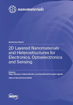
2D Layered Nanomaterials and Heterostructures for Electronics, Optoelectronics and Sensing by Filippo Giannazzo, Federica Bondino, Luca Seravalli, Simonpietro Agnello ISBN 9783725844685, 9783725844678, 3725844682, 3725844674 instant download
This Special Issue aimed to collect contributions on the scalable growth of two-dimensional materials (2DM), on the fabrication approaches of van der Waals (vdW) heterostructures, and on advanced characterization methods and theoretical modelling of these systems. Furthermore, it aimed to address the challenges involved in 2DM integration and device fabrication. Specifically, 10 original research papers have been published covering the following topics:
1. Scalable synthesis of molybdenum disulfide (MoS2) by advanced chemical vapour deposition (CVD) approaches, and by pulsed laser deposition (PLD) on substrates of interest for microelectronics (gallium nitride).
2. First-principles calculations of electronic and optical properties of graphene, borophene, and boron carbide 2D heterostructures.
3. Advanced optical and electronic transport characterization of novel vdW heterostructures.
4. Electronic and optoelectronic devices based on 2DM heterostructures, i.e., novel 2D field effect transistors with vdW contacts; bipolar transistors based on a MoS2/WSe2/MoS2 heterostructure; photo-transistors and self-powered photodetectors based on graphene/Si, and NiO/graphene/Si junctions; photovoltaic devices; biosensors based on MoS2/WTe2 Schottky barriers.
-
This Special Issue provides relevant examples of different ongoing research directions in this expanding field of 2D materials, and it can serve as inspiration for researchers working on these topics.
*Free conversion of into popular formats such as PDF, DOCX, DOC, AZW, EPUB, and MOBI after payment.


